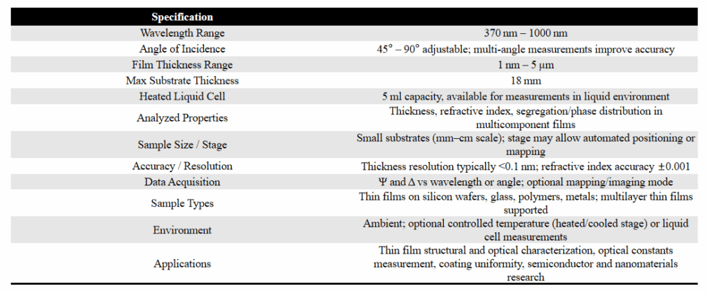
 1. Overview
An Ellipsometer is an optical instrument used to measure the thickness, refractive index, and optical properties of thin films and layered materials. It is a non-destructive, highly sensitive technique widely applied in semiconductor fabrication, coatings, nanomaterials, and surface science. Ellipsometers can analyze single or multilayer films, providing detailed information about film uniformity and composition.
Capabilities
- Thickness range: 1 nm to 5 microns thickness
- Max substrate thickness: 18 mm
- Wavelength: 370-1000 nm, Angle range: 45-90 ˚
- 5 ml Heated liquid cell available
Features
- Analyze thin film’s structural and optical properties
- Thickness, refractive index, segregation characters of multicomponent systems.
2. Principle
Ellipsometry is based on the measurement of changes in the polarization state of light upon reflection from a sample surface:
- Incident light is polarized and directed at the sample at a known angle.
- The reflected light undergoes a change in polarization, described by two parameters: Ψ (amplitude ratio) and Δ (phase difference).
- By analyzing Ψ and Δ, one can calculate the thickness and optical constants (n, k) of the film using models that describe the film-substrate system.
- Different types of ellipsometers include spectroscopic ellipsometers (measuring across a wavelength range) and phase-modulated ellipsometers (high sensitivity to thin films).
3. Data Interpretation
Key data outputs:
- Film Thickness: Derived from the fitted model of Ψ and Δ versus wavelength or angle.
- Refractive Index (n) and Extinction Coefficient (k): Indicate the optical response of the film.
- Film Uniformity & Layer Analysis: Multiple layers can be modeled to extract thickness and optical constants for each layer.
Interpretation Notes:
- Accurate modeling is crucial; known substrate properties improve measurement reliability.
- Deviations between experimental and modeled data can indicate inhomogeneity, roughness, or optical anisotropy.
- Spectroscopic ellipsometry allows determination of dispersion curves and material absorption features.
4. Example Applications
- Semiconductors: Measuring gate oxides, dielectrics, and thin functional layers.
- Coatings: Determining thickness and refractive index of optical or protective coatings.
- Nanomaterials: Characterizing thin films of polymers, metals, or 2D materials.
- Surface Science: Investigating surface functionalization, contamination, or adsorption layers.