1. Overview
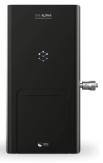
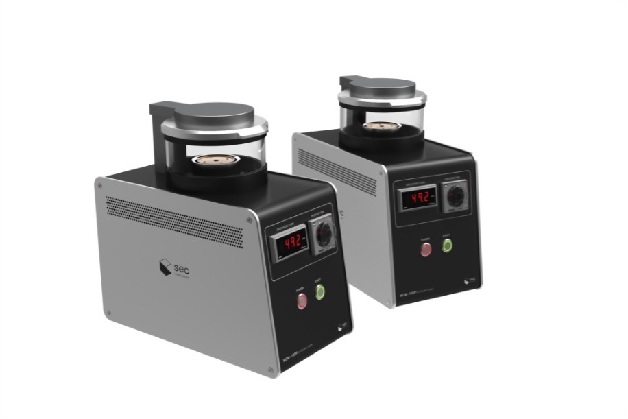
The SNE-Alpha Tabletop Scanning Electron Microscope (SEM) paired with the MCM-100 Ion Sputter Coater is an integrated benchtop solution for high-contrast surface imaging and conductive sample coating. The compact SEM provides fast setup, user-friendly operation, and flexible imaging modes suitable for research laboratories, quality control, and educational environments. The MCM-100 sputter coater enables thin conductive coatings (gold) on non-conductive specimens to prevent charging and improve image quality. Together they deliver a workflow that is optimized for routine morphology inspection, failure analysis, and materials characterization without the footprint or complexity of a full-size SEM system.
Features of SEM:
Features of Ion Sputter Coater
- Use for non-conductive samples to allow imaging without electron charge effects
- Target Materials: Au
2. Principle
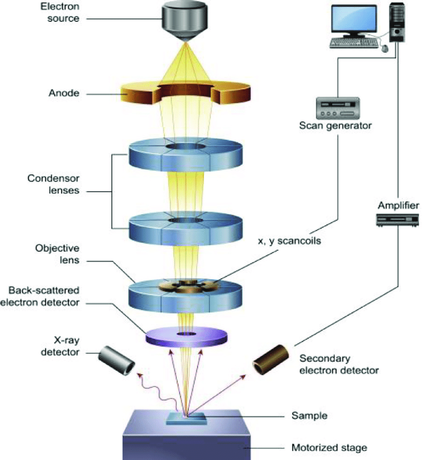
SEM (Scanning Electron Microscope)
- An electron beam is focused and scanned across the sample surface. Interactions between the beam and the specimen produce signals (secondary electrons, backscattered electrons, X-rays) that are collected by detectors to form high-resolution images of surface topography and composition contrast.
- Image contrast arises from topography (secondary electrons) and atomic number or compositional differences (backscattered electrons). Imaging parameters such as accelerating voltage, working distance, beam current, and detector selection control resolution, penetration depth, and contrast.
Ion Sputter Coater (MCM-100)
-
The sputter coater deposits a thin, uniform conductive metal film on samples by ionizing an inert gas (usually argon) and accelerating ions to sputter a metal target. Sputtered atoms condense on the specimen, forming a conductive layer that reduces charging and enhances secondary electron emission. Coating thickness and rate are controlled by current/time settings, allowing very thin coatings for high-resolution imaging of fine features.
3. Data interpretation
- Resolution & Magnification: SEM provides magnified surface images from low to very high magnifications. Interpret features relative to the magnification and the beam interaction volume; very small features may require lower accelerating voltages and thinner conductive coatings to avoid beam penetration or coating masking.
- Topographic Contrast: Bright/dark variations in secondary electron images primarily reflect surface morphology (edges and steep slopes yield stronger secondary-electron signals). Use these images to assess surface texture, particle shape, and microstructural detail.
- Material/Compositional Contrast: Backscattered electron images highlight regions with different mean atomic numbers (heavier elements appear brighter). Compare secondary and backscattered images to separate topographic effects from compositional differences.
- Charging Artifacts: Non-conductive samples that are insufficiently coated or imaged at inappropriate conditions will show bright spots, streaking, or image instability. These artifacts can be reduced by applying a conductive coating (MCM-100) or by lowering beam energy and using environmental/low-vacuum modes if available.
- Measurement Considerations: SEM images are 2D projections of a 3D surface—careful calibration and scale bars are required for any dimensional analysis. Note that coating thickness can alter apparent feature sizes; account for coating when measuring nanoscale features.
- Signal-to-Noise & Beam Damage: Higher beam currents increase signal but may cause beam damage or heating in sensitive materials. Optimize accelerating voltage and dwell time to balance image clarity and sample integrity.
4. Example application
Materials Science: Morphology and microstructure imaging of metals, ceramics, composites, powders, and fracture surfaces.
Nanomaterials: Size, shape and aggregation state analysis of nanoparticles and nanofibers (with appropriate coating and low-voltage imaging).
Polymers & Coatings: Surface texture, coating uniformity, and failure/adhesion analysis after environmental or mechanical testing.
Electronics & Semiconductors: Inspection of circuit features, solder joints, and contamination; defect localization on PCBs and microdevices.
Biological & Life-Science Samples: Surface imaging of biological tissues and cells (typically after dehydration and conductive coating); useful for morphology and micro-structural studies.
Quality Control & Failure Analysis: Routine inspection for contaminants, surface defects, particle contamination, and process verification in industrial settings.
Education & Training: Hands-on SEM imaging for teaching fundamentals of electron microscopy, materials characterization, and sample preparation techniques.